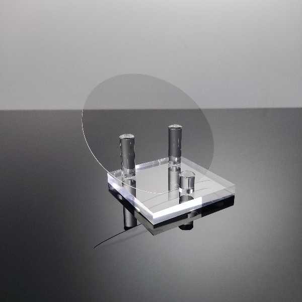
Sapphire (Al2O3) belongs to the hexagonal crystal system, with its crystal orientations typically defined by crystal planes (hkl) and crystal axes (a, b, c). The crystal axes consist of three directions: a, b, and c. Among these, the a and b axes form a 60-degree angle on the plane, while the c axis stands perpendicular to the plane, forming a 120-degree angle. Crystal planes are denoted by Miller indices (hkl), where h, k, and l are integers. In the hexagonal crystal system, common crystal planes of sapphire include {0001}, {1120}, {1102}, among others.
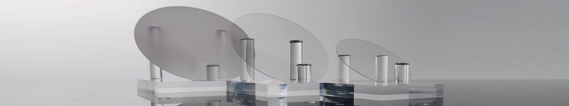
Different crystal orientations of sapphire find specific applications across various domains:
C-plane Sapphire:
Gallium Nitride on Sapphire (GaN on Sapphire) is a key technology in semiconductor manufacturing. GaN, as a wide bandgap third-generation semiconductor, boasts properties such as a wide direct bandgap, robust atomic bonds, high thermal conductivity, excellent chemical stability (virtually impervious to acid corrosion), and strong radiation resistance. These characteristics render it promising for applications in optoelectronics, high-temperature high-power devices, and high-frequency microwave devices. However, due to its high melting point, obtaining large-scale single crystal materials of GaN remains challenging. Therefore, epitaxial growth on alternative substrates such as sapphire wafers is common, demanding substrates of high quality. Compared to other crystal orientations, c-plane sapphire wafers exhibit relatively minimal lattice constant mismatch with III-V and II-VI group deposited films, such as GaN. This, coupled with even smaller lattice constant mismatch with AlN films, makes them favored substrate materials for GaN growth. They find application in the fabrication of white/blue/green LEDs, laser diodes, infrared detectors, etc.

A-plane Sapphire:
Sapphire single crystals, owing to their outstanding overall performance, particularly remarkable transparency, serve as ideal mid-infrared window materials, enhancing the penetration effect of infrared rays, thus finding widespread use in military optoelectronic devices. Among these, A-plane sapphire represents a polar surface (C-plane) normal direction, being non-polar. Generally, sapphire crystals grown in the a direction exhibit superior quality to those in the c direction, boasting fewer defects, less inclusion structures, and a more complete crystal structure, consequently offering improved light transmission performance. Moreover, owing to the Al-O-Al-O atomic bonding on the A-plane, a-plane sapphire demonstrates significantly higher hardness and wear resistance than c-plane sapphire. Consequently, A-plane chips are predominantly employed as window materials. Additionally, A-plane sapphire demonstrates uniform dielectric constant and high insulation characteristics, making it suitable for hybrid microelectronics technology and growth of high superconductors. For instance, it is used in the growth of heteroepitaxial superconducting films on composite substrates of sapphire and cerium oxide (CeO2). However, processing challenges arise due to the substantial bond energy of Al-O.
R-plane Sapphire:
The R-plane represents the non-polar surface of sapphire, endowing sapphire devices with varied mechanical, thermal, electrical, and optical properties based on R-plane position variations. Typically, R-plane sapphire substrates are preferred for silicon heterogeneous epitaxial deposition, primarily utilized in semiconductor, microwave, and microelectronic integrated circuit applications. Presently, with the proliferation of smartphones and tablet computer systems, R-plane sapphire substrates have supplanted existing compound SAW devices in smartphones and tablets, providing a substrate for devices capable of enhancing performance.
M-plane Sapphire:
The M-plane denotes the semi-polar surface of sapphire. Due to the promising application prospects of sapphire in blind UV detection, wide-bandgap MgZnO alloy semiconductor thin films are garnering increasing attention. A range of MgxZn1-xO films with diverse compositions are prepared on M-plane (10-10) sapphire wafers utilizing the low-pressure metal organic chemical vapor deposition (LP-MOCVD) technique. In specific experiments or studies, m-plane sapphire may find utility in testing the electrical, optical, or magnetic properties of sapphire or in specialized material growth research.
These applications underscore the significance and versatility of different crystal orientations of sapphire across LED manufacturing, semiconductor growth, optical devices, and scientific research domains. Consequently, comprehending crystal orientations is imperative for achieving the desired performance when selecting sapphire for specific applications.
Related product links
As semiconductor technology advances, Gallium Nitride (GaN) has become a core material in optoelectronics, rad...
With the rapid advancement of third-generation semiconductor technologies, Silicon Carbide (SiC) has emerged a...
As third-generation semiconductor materials such as silicon carbide (SiC) and gallium nitride (GaN) continue t...