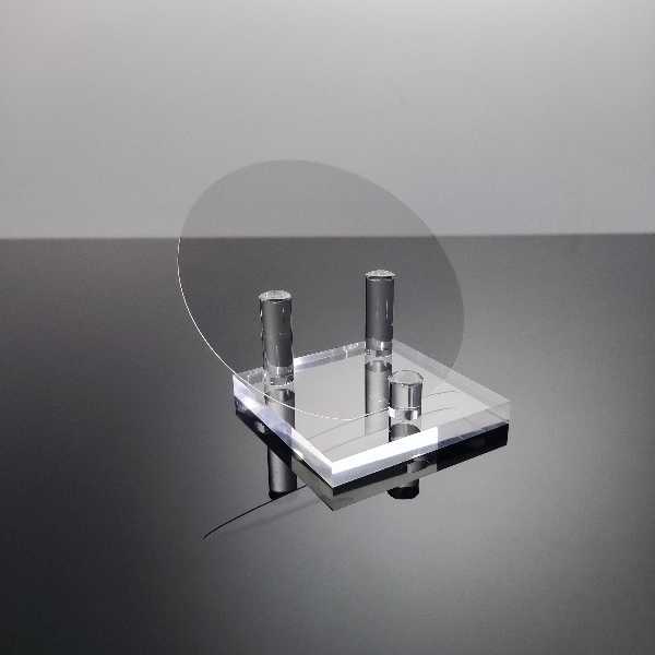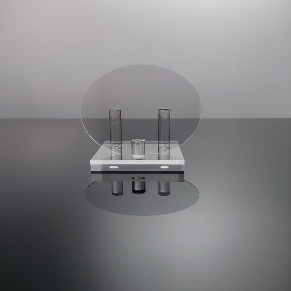
| Item | Sapphire Substrate(1~8inch) | ||||||
| Diameter | 25.4±0.1mm | 50.8±0.1mm | 76.2±0.2mm | 100.0±0.2mm | 125.0±0.3mm | 150.0±0.3mm | 200.0±0.5mm |
| Thickness | 430±25μm | 430±25μm | 500±25μm | 650±25μm | 800±25μm | 1000±25μm | 1600±25μm |
| Surface Orientation | C-plane (0001) off-angle toward M-axis(10-10) 0.2 ± 0.1° | ||||||
| C-plane (0001) off-angle toward A-axis(11-20) 0 ± 0.1° | |||||||
| Primary Flat Orientation | A-Plane (11-20) ± 1.0° | ||||||
| Primary Flat Length | 8.0±1.0mm | 16.0±1.0mm | 22.0±1.0mm | 30.0±1.0mm | 30.0±2.0mm | 47.5±2.0mm | Notch |
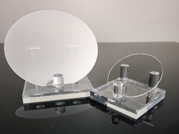
| Front Surface Finish | Epi-polished,Ra<0.3nm | ||||||
| Back Surface Finish | SSP:Fine-ground,Ra=0.8-1.2μm; DSP:Epi-polished,Ra<0.3nm | ||||||
| Laser Mark | Back side | ||||||
| TTV | ≤5μm | ≤8μm | ≤10μm | ≤10μm | ≤15μm | ≤20μm | ≤30μm |
| BOW | ≤8μm | ≤10μm | ≤12μm | ≤15μm | ≤25μm | ≤25μm | ≤40μm |
| WARP | ≤10μm | ≤12μm | ≤15μm | ≤20μm | ≤30μm | ≤30μm | ≤60μm |
| Edge Exclusion | ≤2 mm | ||||||
Customization specifications:
* Various orientations such as A/R/M/N Plane, C off M(1°-10°), C off A(1°-10°).
* Various sizes and shapes such as 10*10mm,12inch
* Various thicknesses:0.1~20mm
* Various surface roughness such as slicing,lapping,polishing.
* Sapphire crystal ingots are available.
The sapphire is a crystalline form of aluminum oxide(α-Al2O3) with a hexagonal structure, which is composed of three oxygen atoms and two aluminum atoms combined by covalent bonds. The chemical properties of sapphire crystal are very stable, insoluble in water, and excellent corrosion resistance to strong acids and strong alkalis. The sapphire crystal has a high hardness of 9 on the Mohs scale, a melting point of 2050°C, a boiling point of 3500°C, and a maximum working temperature of 1900°C. Sapphire wafer has high light transmission,low thermal conductivity,good electrical insulation,excellent mechanical properties, and good wear resistance and scratch resistance.
| Crystal Structure | Hexagonal |
| Lattice Constant(nm) | a=4.76Å c=12.99Å |
| Density(g/cm3) | 3.98 |
| Melting point(℃) | 2040 |
| Mohs Hardness(mohs) | 9 |
| Dielectric Constant | 9.3(A plane) |
| 11.5(C plane) | |
| Thermal Conductivity(W/cm.K) | 0.46 |
| Thermal Expansion | 6.7*10-6/k(C plane) 5.0*10-6/k(A plane) |
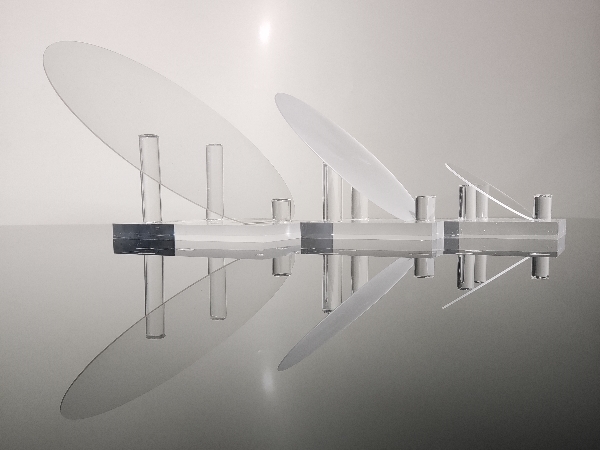
| Refractive Index | 1.762-1.777 |
| Transmission | Test sample:Sapphire:D76.2*4mm |
| UV:200~380nm 74%~84% | |
| Visible light:380~760nm 85% | |
| Infrared:760~1000nm 85% | |
| Far-Infrared:>1000nm 80%~100% |