


| Item | Patterned Sapphire Substrate(2~6inch) | ||
| Diameter | 50.8 ± 0.1 mm | 100.0 ± 0.2 mm | 150.0 ± 0.3 mm |
| Thickness | 430 ± 25μm | 650 ± 25μm | 1000 ± 25μm |
| Surface Orientation | C-plane (0001) off-angle toward M-axis (10-10) 0.2 ± 0.1° | ||
| C-plane (0001) off-angle toward A-axis (11-20) 0 ± 0.1° | |||
| Primary Flat Orientation | A-Plane (11-20) ± 1.0° | ||
| Primary Flat Length | 16.0 ± 1.0 mm | 30.0 ± 1.0 mm | 47.5 ± 2.0 mm |
| R-Plane | 9-o'clock | ||
| Front Surface Finish | Patterned | ||
| Back Surface Finish | SSP:Fine-ground,Ra=0.8-1.2um; DSP:Epi-polished,Ra<0.3nm | ||
| Laser Mark | Back side | ||
| TTV | ≤8μm | ≤10μm | ≤20μm |
| BOW | ≤10μm | ≤15μm | ≤25μm |
| WARP | ≤12μm | ≤20μm | ≤30μm |
| Edge Exclusion | ≤2 mm | ||
| Pattern Specification | Shape Structure | Dome, Cone,Pyramid | |
| Pattern Height | 1.6~1.8μm | ||
| Pattern Diameter | 2.75~2.85μm | ||
| Pattern Space | 0.1~0.3μm | ||
Customization specifications:
* Nanometer patterned sapphire substrate(NPSS).
* Sapphire PSS of various orientations.
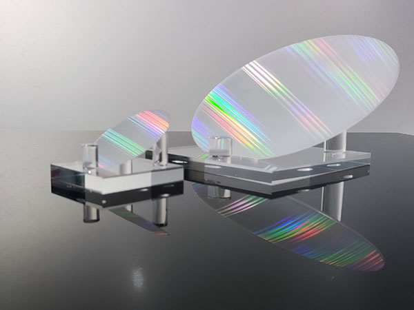
Patterned sapphire substrate(PSS) is a process of making some specific micrometer pattern like Dome,Cone or Pyramid-shaped on the sapphire substrate.Uneven patterns on sapphire substrates can generate light scattering or refraction,thereby improving the luminous efficiency.
| Crystal Structure | Hexagonal |
| Lattice Constant(nm) | a=4.76Å c=12.99Å |
| Density(g/cm3) | 3.98 |
| Melting point(℃) | 2040 |
| Mohs Hardness(mohs) | 9 |
| Dielectric Constant | 9.3(A plane) 11.5(C plane) |
| Thermal Conductivity(W/cm.K) | 0.46 |
| Thermal Expansion | 6.7*10-6/k(C plane) 5.0*10-6/k(A plane) |
| Refractive Index | 1.762-1.777 |
| Transmission | Test sample:Sapphire:D76.2*4mm |
| UV:200~380nm 74%~84% | |
| Visible light:380~760nm 85% | |
| Infrared:760~1000nm 85% | |
| Far-Infrared:>1000nm 80%~100% |