
| Item | Diamond Substrate | |
| Diameter | 25.4±0.3mm | 50.8±0.5mm |
| Thickness | 450±30μm | 450±30μm |
| Growth Method | MPCVD | |
| Front Surface Finish | Polished,Ra<1.0 nm | |
| Back Surface Finish | Polished; Grinding | |
| Thermal expansivity | 1.3 (10-6K-1) | |
| Thermal coefficient | 1000-2000W/m.K | |
| TTV | ≤5 mm | ≤10 mm |
| Edge Exclusion | ≤3 mm | |
Customization specifications:
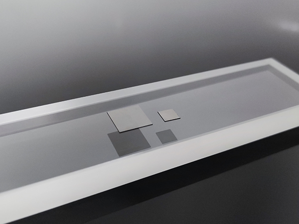
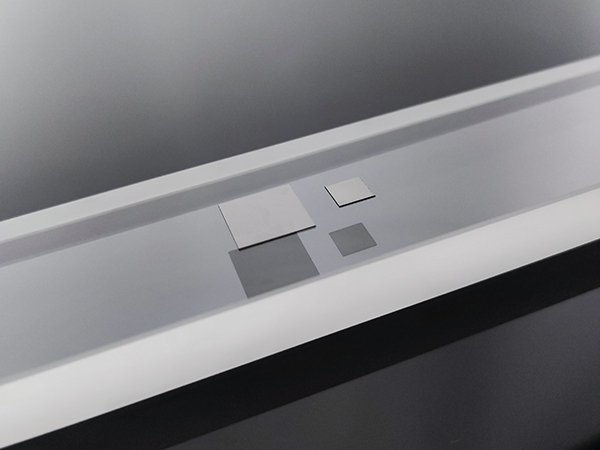
* Various sizes and shapes such as 5*5mm,10*10mm,1~4inch.
* Various thicknesses:0.1~5mm
* Various surface roughness such as slicing,lapping.
* crystal type:single crystal diamond or polycrystalline diamond.
Diamond is the hardest substance in the world and it is gaining more attention for its outstanding optical, electrical, mechanical, and thermal properties. Artificial diamond can be grown by MPCVD.In this process diamond is grown by starting with a carbon containing gas like methane and hydrogen, then carbon atoms are created by high pressure and high temperature,which is responsible for the deposition on the substrates to form diamond single crystal.
| Crystal Structure | Cubic |
| Lattice Constant(nm) | 0.3567Å |
| Density(g/cm3) | 3.52 |
| Melting point(℃) | 3550 |
| Mohs Hardness(mohs) | 10 |
| Dielectric Constant | 5.68 |
| Band Gap(eV) | 5.47 |
| Breakdown Electrical Field (MV/cm) | 10 |
| Thermal Conductivity(W/cm.K) | 12-18 |
| Thermal Expansion | 3.196*10-6/k |
| Refractive Index | 2.417 |